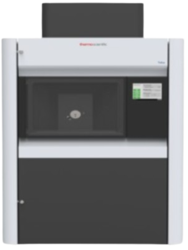
Transmission Electron Microscopy (TEM) is a powerful technique for visualizing and analyzing materials at the atomic level. Developed in the 1930s by Ernst Ruska and Max Knoll, it overcame the limitations of optical microscopes and has since become essential in both research and industry.
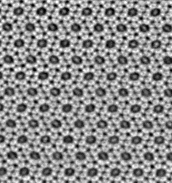
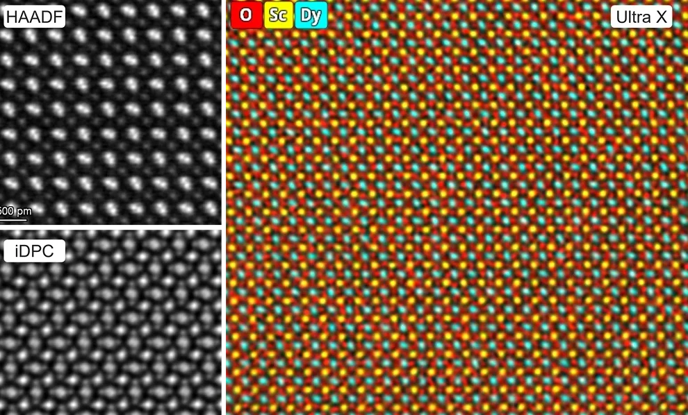
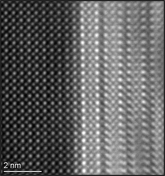
TEM works by transmitting electrons through an ultra-thin specimen. These electrons interact with the material’s internal structure, producing highly detailed images with sub-nanometer resolution, allowing observation of individual atoms and molecular structures. Beyond imaging, TEM also provides insights into crystal structure, composition, and defects.
TEM has wide-ranging applications: studying metals, alloys, polymers, and nanomaterials in materials science; exploring cells and viruses in biology; analyzing thin films in semiconductor research; and examining catalysts in chemistry. In both academic and industrial settings, TEM is a key tool for uncovering intricate details in samples.
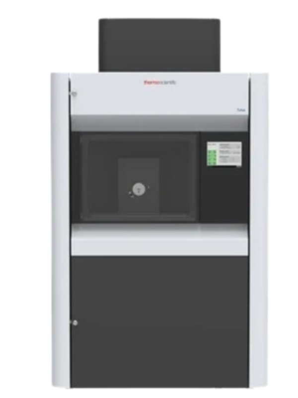
Its atomic-level resolution and analytical power make TEM one of the most advanced microscopy techniques today. It offers users profound insights into material properties, driving innovation in scientific research and technology development. Investing in TEM unlocks discoveries beyond the capabilities of conventional microscopes.